My research as a graduate student focuses on biosensing applications using electrochemical impedimetric methods. Unlike mechatronic systems, these applications consider a dynamic environment at such a microscale, it is quite hard to perceive what is really going on when we merely recognize the change of physical property. I usually ask myself: What is the underlying mechanism? Tucked away from the limit of horizon of the human eye, we often see nothing happening when doing these experiments.
That is why simulation is so important! In this project, I performed 3 simulation tasks in order to visualize the changes of important physical properties for my study (impedimetric microfluidic chip for biosensing) using COMSOL Multiphysics.
The tasks are:
- Velocity field simulation inside microfluidic channel.
- Real-time molecule immobilization on gold surface.
- Electrochemical impedance spectroscopy (EIS) simulation.
The result of task 1 supports the hypotheses of task 2 and 3.
Physical Environment Setting
The simulation environment is set as the interior of a microfluidic channel with gold microelectrodes. See the film below for visualization.
The chip is fabricated using soft lithography and photolithography. The microfluidic channel has a width of 1mm and a height of 100μm at the center. The gold microelectrodes form a pair for square pads (300×300μm) at the center of the channel (Fig. 1).

Figure 1. Microfabrication process, dimensions, and microscopic view of the microfluidic electrode chip used in this project.
Velocity Field Simulation Inside Microfluidic Channel
The objective of this task is to simulate the fluid velocity field inside the channel on a sliced plane. Due to the fact that 3D simulation is time-consuming, if a 3D environment can be reduced to a 2D environment, then a large amount of time can be saved. By performing this task, it can be seen if dimension reduction modeling of task 2 and 3 are feasible.
Considering the physical nature of the microfluidic channel, a laminar flow model is implemented along with the Navier-Stokes equation:
$$\rho(\textbf{u}\cdot\nabla)\textbf{u}=\nabla\cdot[-pI+\mu(\nabla \textbf{u}+(\nabla \textbf{u})^T)]+F$$
, which means a balance between inertia (\(\rho(\textbf{u}\cdot\nabla)\textbf{u}\)), pressure (\(-pI\)), viscous (\(\mu(\nabla \textbf{u}+(\nabla \textbf{u})^T)\)) and external (\(F\)) forces. A stationary study is implemented (\(\rho \nabla \cdot \textbf{u}=0\)), and water is set as the fluid.
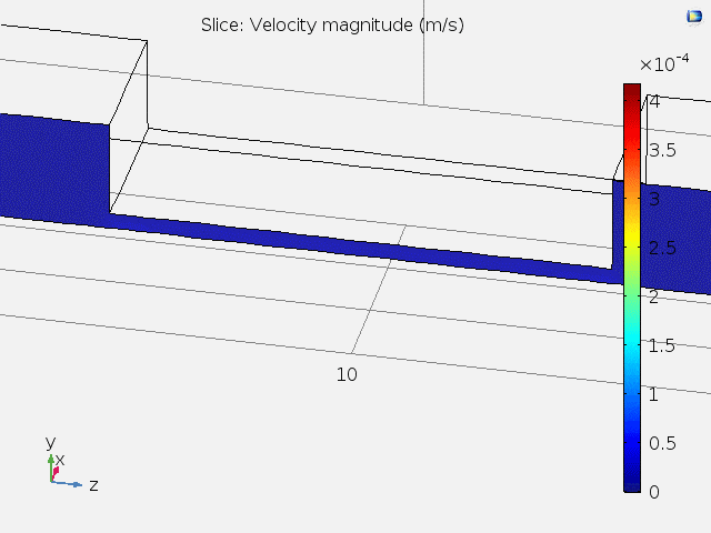
Fig. 2 shows the 3D velocity field inside the channel. A bigger arrow indicates a larger velocity magnitude. The reason that the velocity is faster at the center is because of the lower channel height.

Figure 2. 3D velocity field inside microfluidic channel.
Fig. 3 shows animated 2D velocity fields of sliced planes inside the channel. Due to laminar flow, velocities near the boundary get close to zero. However, the steady-state velocity reaches a constant value away from the boundary.


Figure 3. 2D velocity fields for xy and zy sliced planes.
A top view of the velocity field and the velocity at different x positions are shown in Fig. 4. It can be concluded that at the center of the channel where the microelectrodes lie, the fluid velocity stays constant, and subsequent tasks can be carried out using 2D models.

Figure 4. Top-view and x position-dependent velocity magnitude of fluid.
Real-time Molecule Immobilization on Gold Surface.
For microfluidic electrochemical biosensors, it is quite common that immobilization of sensing elements takes place at the center of the channel on electrode surfaces (e.g. Au). In this task, molecules are simulated to flow past the channel, and be immobilized on the electrode pad at the bottom center. A slice on the zy plane is used as the modeling geometry of this task (Fig. 5).

Figure 5. Modeling geometry used in task 2. A sliced area of the microfluidic channel with pad electrode at the bottom center is used.
Here, the molecules convect and diffuse near the surface, the rate of immobilization is determined by several factors including the inlet concentration (c0), diffusion coefficient (D), maximum surface molecule density (Γs). The convection-diffusion equation and transport-adsorption equation are used along with time-dependent study:
$${{\partial c} \over {\partial t}} + \nabla \cdot (-D\nabla c) + \textbf{u} \cdot \nabla c = R$$
$${{\partial c_s} \over {\partial t}} + \nabla \cdot (-D\nabla c_s) = k_{ads} c(\Gamma_s – c_s)-k_{des} c_s$$
For the transport-adsorption equation, it is assumed that the change of surface concentration plus the rate of surface diffusion equals the rate of Langmuir adsorption isotherm.
Fig. 6 shows the time-dependent surface concentration (cs) change when c0 = 1μM, and Fig. 7 shows the binding curve (probe density vs time) for different values of c0.

Figure 6. Time-dependent surface concentration (cs) change. t = 0~18hr.

Figure 7. Probe surface density (molecules/cm2) vs time (hr).
At concentrations above 0.1μM, the probe density almost saturates to a value of 9.6×10¹² molecules/cm2 before immobilizing for 10 hours. The result highly resembles a typical binding curve, suggesting the possibility for computer simulating assisted optimization of in vitro parameters, which is really helpful for understanding underlying mechanisms for the system.
Electrochemical Impedance Spectroscopy (EIS) Simulation.
EIS is a rapid and label-free method for detection of bio-molecules, and is widely implemented on a variety of biosensors. In this task, I simulated EIS diagrams by changing the values of the heterogeneous rate constant (k0) and the double layer capacitance (Cdl). Both Cdl and k0 are affected by the immobilized surface molecule density on an electrode surface, and are important physical properties when analyzing EIS data. A slice on the xy plane is used as the modeling geometry of this task (Fig. 8).

Figure 8. Geometry being simulated for task 3. A 2D plane is sliced in the xy direction.
Here, a sinusoidal voltage wave is applied between the two electrodes (amplitude ≅ 5mV), and Bode plots and Nyquist plots can be drawn according to the measured impedance. According to the surface redox reaction, an equivalent circuit can be constructed. The equivalent circuit for this task is shown in Fig. 9.

Figure 9. Equivalent circuit used in my research and task 3.
Fick’s 2nd law and Butler-Volmer equation are used for simulation:
$${{\partial c}\over{\partial t}} = \nabla \cdot (D\nabla c)$$
$$j = nFk_0 (c_{Red} e^{ {(n-\alpha_c)F\eta} \over {RT} } – c_{Ox} e^{ {-\alpha_c F\eta} \over {RT} })$$
EIS plots are simulated for different values of k0 and Cdl (Fig. 10).

Figure 10. Bode and Nyquist plots for the simulated EIS data. k0 has a range from 0.001 to 0.1 (cm/s), and Cdl has a range from 0.01 to 100 (uF/cm2).
By undergoing this simulation project, I furthermore understood some fundamental interactions between the physical properties and outcome of my research to a new depth, and developed new concepts about how to improve it.
After completing this project, I also used COMSOL for simulating time-dependent concentration gradient variation of redox molecules in my 1st author journal paper “Diffusion impedance modeling for interdigitated array electrodes by conformal mapping and cylindrical finite length approximation”.